Board Overview
The Companion Board is based around the LMS8001A RFIC, which shifts RF analog signals from one frequency range to another. Usually, the lower frequency range is designated as IF, while the higher frequency range is designated as RF.
A block diagram for LMS8001 Companion Board is presented in Figure 2.

Figure 2. LMS8001 Companion 3v2 block diagram.
Components
This section provides an overview of the main components on the LMS8001 Companion Board. A top view is shown in Figure 3 and reverse in Figure 4.
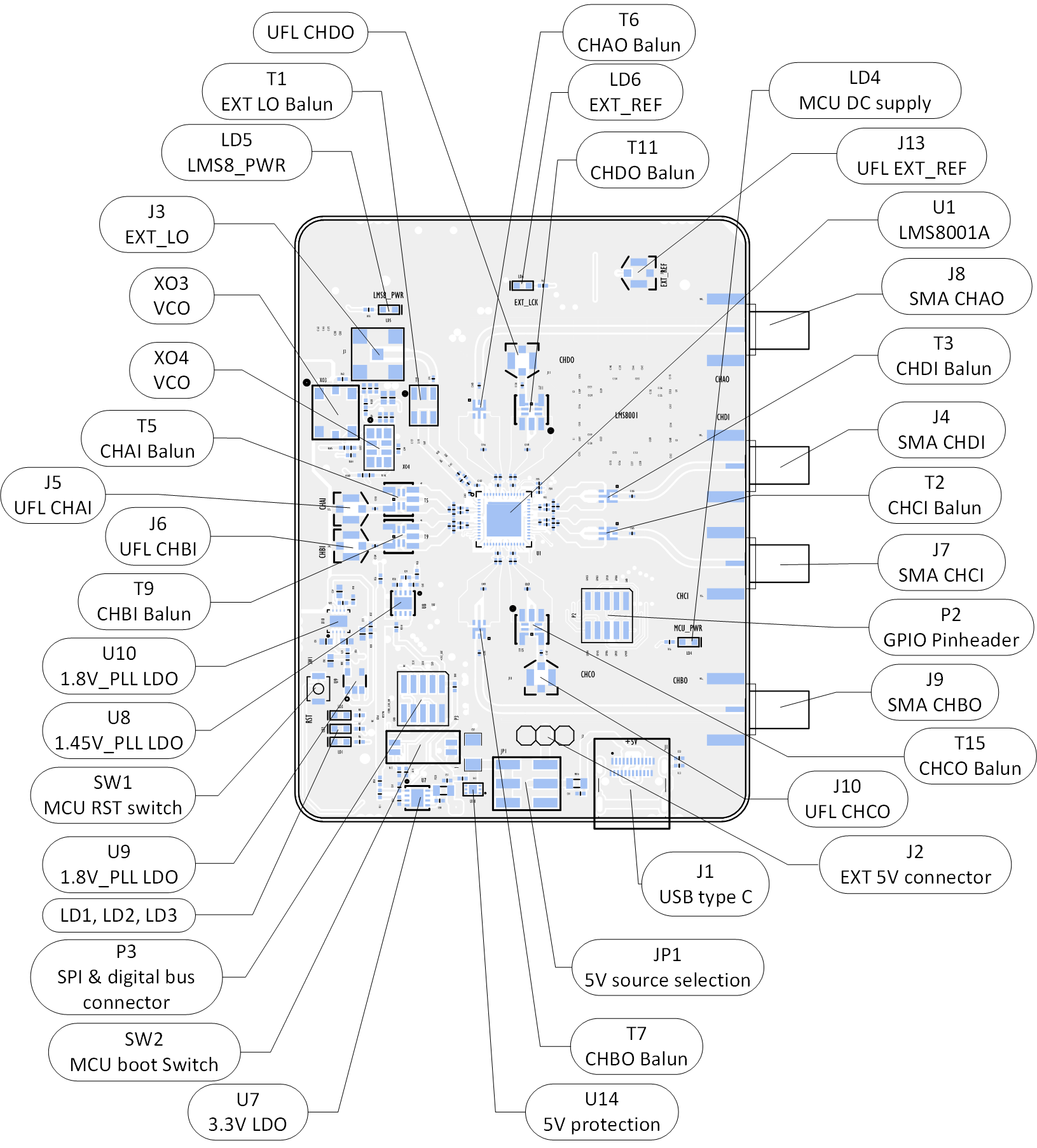
Figure 3. LMS8001 Companion 3v2 top connectors and main components.
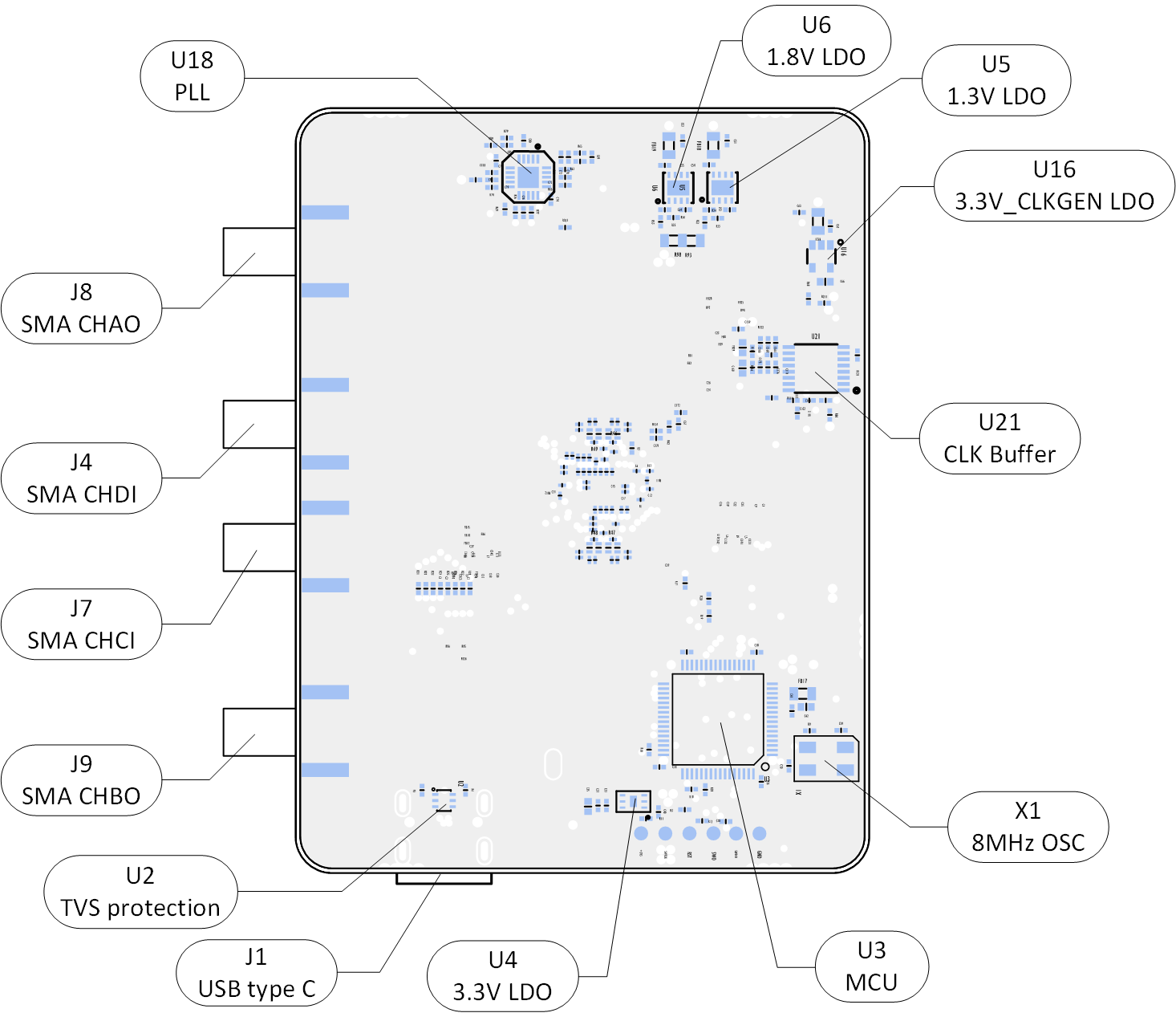
Figure 4. LMS8001 Companion 3v2 reverse connectors and main components.
A description of the components is given in Table 1.
Board Reference |
Type |
Description |
|---|---|---|
RF Block |
||
U1 |
RF mixer |
Lime Microsystems LMS8001A |
J3 |
SMA |
External LO signal connector |
J4 |
SMA |
CHDI connector |
J5 |
UFL |
CHAI connector |
J6 |
UFL |
CHBI connector |
J7 |
SMA |
CHCI connector |
J8 |
SMA |
CHAO connector |
J9 |
SMA |
CHBO connector |
J10 |
UFL |
CHCO connector |
J11 |
UFL |
CHDO connector |
T1 |
4.5-3500 MHz balun |
External LO signal balun, Minicircuits TC1-1-13M+ |
T2 |
3.5-11 GHz balun |
CHCI balun, Minicircuits NCR2-113+ |
T3 |
3.5-11 GHz balun |
CHDI balun, Minicircuits NCR2-113+ |
T5 |
4.5-3500 MHz balun |
CHAI balun, Minicircuits TC1-1-13M+ |
T6 |
3.5-11 GHz balun |
CHAO balun, Minicircuits NCR2-113+ |
T7 |
3.5-11 GHz balun |
CHBO balun, Minicircuits NCR2-113+ |
T9 |
4.5-3500 MHz balun |
CHBI balun, Minicircuits TC1-1-13M+ |
T11 |
4.5-3500 MHz balun |
CHDO balun, Minicircuits TC1-1-13M+ |
T15 |
4.5-3500 MHz balun |
CHCO balun, Minicircuits TC1-1-13M+ |
PLL Block |
||
J13 |
UFL |
External reference signal connector |
U18 |
PLL |
ADI ADF4002 |
U21 |
Clock buffer |
Onsemi NB3H83905C |
XO3 |
40 MHz VCO |
Racon E6245LF |
XO4 |
40 MHz VCO |
Racon RTX5032A |
LD6 |
LD indicator |
Indicator of REF CLK signal (lock detected) |
DC Supply Block |
||
JP1 |
6 Pin header |
Selection of 5V supply |
J2 |
3 Pin header |
EXT 5V connector |
U4 |
3.3V LDO |
LDO for 3.3 V |
U5 |
1.3V LDO |
LDO for 1.3 V |
U6 |
1.8V LDO |
LDO for 1.8 V |
U7 |
3.3V LDO |
LDO for 3.3 V |
U8 |
1.45V_PLL LDO |
LDO for PLL 1.45 V |
U9 |
1.8V_PLL LDO |
LDO for PLL 1.8 V |
U10 |
1.8V_PLL LDO |
LDO for PLL 1.8 V |
U14 |
5V protection |
|
U16 |
3.3V_CLKGEN LDO |
LDO for PLL 3.3 V |
LD5 |
LED indicator |
Indicator of 5V signal |
MCU and Communication Block |
||
U3 |
MCU |
STM32F105RBT6 |
U2 |
TSV protection |
TSV protection for USB data lines |
J1 |
USB type C |
USB connector for communication and DC supply |
X1 |
Ext. osc. for MCU |
8 MHz crystal oscillator |
SW1 |
MCU reset switch |
|
SW2 |
MCU boot switch |
|
P2 |
10 Pin header |
GPIO lines |
P3 |
10 Pin header |
SPI and digital control signals |
LD1 |
MCU LED |
MCU programable indicator |
LD2 |
MCU LED |
MCU programable indicator |
LD3 |
MCU LED |
MCU programable indicator |
LD4 |
LED indicator |
Indicator of MCU DC power signal |